Do you need help learning for your NCERT Class 12 Physics exam? Students may want to download NCERT MCQ Questions for Class 12 Physics Chapter 14 Semiconductor Electronics: Materials, Devices and Simple Circuits with Answers Pdf free download. These Semiconductor Electronics: Materials, Devices, and Simple Circuits Class 12 MCQs Questions with Answers can help understand the concepts score better in your Class 12 Physics Exam, so make sure you practice these! Check out chapter-wise MCQ Questions for Class 12 Physics with Answers.
Semiconductor Electronics: Materials, Devices and Simple Circuits Class 12 MCQs Questions with Answers
Solve these Semiconductor Electronics: Materials, Devices and Simple Circuits Multiple Choice Questions of Class 12 Physics Chapter 14 MCQ, so as not to miss out on any concept from being clear about what they mean!
I. Choose the correct answer
Question 1.
In the figure, assuming the diodes to be ideal,
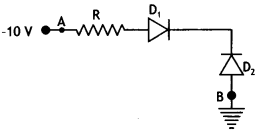
(a) D1 is forward biased and D2 is reverse biased and hence current flows from A to B.
(b) D2 is forward biased and D1 is reverse biased and hence no current flows from B to A and vice versa.
(c) D1 and D2 are both forward biased and hence current flows from A to B.
(d) D1 and D2 are both reverse biased and hence no current flows from A to B and vice versa.
Answer
Answer: (b) D2 is forward biased and D1 is reverse biased and hence no current flows from B to A and vice versa.
Question 2.
Hole is
(a) an anti-particle of electron.
(b) a vacancy created when an electron leaves a covalent bond.
(c) absence of free electrons.
(d) an artificially created particle.
Answer
Answer: (b) a vacancy created when an electron leaves a covalent bond.
Question 3.
For the depletion region of a diode which one is incorrect?
(a) There are no mobile charges.
(b) Equal number of holes and electrons exists, making the region neutral.
(c) Recombination of holes and electrons has taken place.
(d) Immobile charged ions exist.
Answer
Answer: (a) There are no mobile charges.
Question 4.
To reduce the ripples in a rectifier circuit with capacitor filter which one is false?
(a) RL should be increased.
(b) Input frequency should be decreased.
(c) Input frequency should be increased.
(d) Capacitors with high capacitance should be used.
Answer
Answer: (b) Input frequency should be decreased.
Question 5.
Carbon, silicon and germanium have four valence electrons each. These are characterised by valence and conduction bands separated by energy band gap respectively equal to (Eg)C, (Eg)Si and (Eg) Ge. Which of the following statements is true?
(a) (Eg)Si < (Eg)Ge < (Eg)C
(b) (Eg)C < (Eg)Ge > (Eg)Si
(c) (Eg)C > (Eg)Si > (Eg)Ge
(d) (Eg)C = (Eg)Si = (Eg)Ge
Answer
Answer: (c) (Eg)C > (Eg)Si > (Eg)Ge
Question 6.
In an unbiased p-n junction, holes diffuse from the p-region to n-region because
(a) free electrons in the n-region attract them.
(b) they move across the junction by the potential difference.
(c) hole concentration in p-region is more as compared to n-region.
(d) All the above.
Answer
Answer: (c) hole concentration in p-region is more as compared to n-region.
Question 7.
In a p-n junction diode, change in temperature due to heating:
(a) affects only reverse resistance
(b) affects only forward resistance
(c) Does not affect resistance of p-n junction
(d) affects the overall V-I characteristics of p-n junction
Answer
Answer: (d) affects the overall V-I characteristics of p-n junction
Question 8.
A specimen of silicon is to be made p-type semiconductor for this one atom of indium, on an average, is doped in 5 × 10⁷ silicon atoms. If the number density of silicon is 5 × 10²² atoms m-3, then the number of acceptor atoms per cm³ will be
(a) 2.5 × 1030
(b) 1.0 × 10¹³
(c) 1.0 × 10¹⁵
(d) 2.5 × 1036
Answer
Answer: (c) 1.0 × 10¹⁵
Question 9.
The given circuit has two ideal diodes connected as shown in the figure below. The current flowing through the resistance R1 will be:
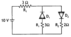
(a) 1.43 A
(b) 3.13 A
(c) 2.5 A
(d) 10.0 A
Answer
Answer: (c) 2.5 A
Question 10.
Consider the junction diode as ideal. The value of current flowing through AB is:
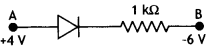
(a) 0 A
(b) 10-2A
(c) 10-1 A
(d) 10-3 A
Answer
Answer: (b) 10-2A
II. Fill in the blanks
Question 1.
At room temperature …………………… is the energy gap for silicon.
Answer
Answer: 1.12 eV
Question 2.
A pure semiconductor which is free of impurity is called …………………… semiconductor.
Answer
Answer: Intrinsic
Question 3.
When an impurity is added to a pure semiconductor it becomes …………………… semiconductor.
Answer
Answer: Extrinsic
Question 4.
There are …………………… types of extrinsic semiconductors.
Answer
Answer: Two
Question 5.
Mobility of hole is …………………… than that of electrons.
Answer
Answer: Less
Question 6.
…………………… is deliberate addition of desirable impurity atoms into an intrinsic semiconductor to increase its electrical conductivity.
Answer
Answer: Doping
Question 7.
…………………… type is obtained by doping an intrinsic semiconductor with a pentavalent impurity.
Answer
Answer: n
Question 8.
…………………… type is obtained by doping an intrinsic semiconductor with a trivalent impurity.
Answer
Answer: P
Question 9.
…………………… are the majority carriers in N-type semiconductor.
Answer
Answer: Electrons
Question 10.
…………………… are the majority carriers in P-type semiconductor.
Answer
Answer: Holes
Question 11.
Two important processes that occur during the formation of a p-n junction are …………………… and ……………………
Answer
Answer: diffusion and drift
Question 12.
The …………………… is the fictitious battery, which seems to be connected across the junction with its positive terminal in the n-region and the negative terminal in the p-region.
Answer
Answer: potential barrier
Question 13.
The region around the junction, which is devoid of any mobile charge carriers, is called the ……………………
Answer
Answer: depletion layer or region
Question 14.
In p-n junction diode there is a …………………… of majority carriers across the junction in forward bias.
Answer
Answer: Diffusion
Question 15.
A p-n junction is said to be …………………… based if the p-type semiconductor is connected to the positive terminal and the n-type semiconductor is connected to the negative terminal of an external battery.
Answer
Answer: Forward
Question 16.
The resistance of p-n junction is …………………… when reverse biased.
Answer
Answer: High
Question 17.
A …………………… is a device, which converts ac into pulsating dc, i.e. unidirectional current.
Answer
Answer: rectifier
Question 18.
The output frequency of the half wave rectifier is …………………… as the input frequency.
Answer
Answer: same
Question 19.
LED works under …………………… bias.
Answer
Answer: Forward
Question 20.
The Zener diode is always …………………… biased.
Answer
Answer: reverse
Question 21.
A photo diode is always …………………… biased.
Answer
Answer: 1.8 eV
Question 22.
The semiconductor used for fabrication of visible LEDs must at least have a band gap of ……………………
Answer
Answer: Reverse
This NCERT MCQ Questions for Class 12 Physics Chapter 14 Semiconductor Electronics: Materials, Devices and Simple Circuits with Answers Pdf free download have been put together to help students understand the CBSE Class 12 Physics Semiconductor Electronics: Materials, Devices and Simple Circuits MCQs Multiple Choice Questions with Answers. Hope you found this helpful!